Home - About AR - Learning Material - Exams - Clubs - Posters
These are circuits which use two states, 0 and 1.
Modern TTL and CMOS generally use positive logic, with a voltage near the positive rail for 1, and a voltage close to ground for 0.
Now off the exam, some systems invert this, which is called negative logic. A few systems use negative voltages.
Some oscillators automatically switch an output between high and low and back again, repeating this forever. These are called "astable", as they have no stable state. Other terms are multivibrator, or "astable multivibrator".
Others respond to an input pulse by either transitioning the output from low to high, or low to high, then returning to the original state after a certain period. Having one stable state, these are this termed "monostable".
The 555 timer can be configured to do either. In these devices resistor-capacitor time constants are used. For higher frequencies crystals can be used if stability is needed, and there are ICs which, say use a 3.58 MHz "colorburst" crystal, and divide this down to 60 Hz.
A variation is an IC which a has two stable states, so is termed "bi-stable". States change in response to a an input pulse, and this is called a flip-flop, because it flips and flops between two states. Other versions had Set and Reset inputs; or a Data input which allows the state on the input line to be stored in response to an enable pulse. Each flip-flop is a single bit of memory.
A single flip-flop performs a divide by two function, so if we wish to divide the frequency by 4, we need 2 flip-flops (and many IC packages give you exactly this).
These devices increment outputs in response to an input pulse. A famous example is the 4017, which can step through 10 outputs, before returning to the first, as well as having a "carry" output, so functioning as a decade counter, generating one pulse for every 10 pulses on the input.
Others increment a 4 digit binary counter, or a BCD counter, etc.
While there are versions with more inputs, the classic version had 2 inputs and a single output. Thus a 14 pin DIP package can contain 4 gates (plus the positive and ground power connections).
The simplest gates are inverters, also called NOT gates, as a 0 in results in a 1 out, and a 1 in results in a 0 out.
The standard versions are AND, OR, NAND, NOR. And means both inputs must be high to generate a high output, while with an OR, only one need be high, but this also applies of both are high. An N at the beginning of the name indicates that the output is inverted.
A variation is the X-OR gate, and the X-NOR. This is the Exclusive-OR, meaning that if one or other input is high, then the output is high, but if both are high, the output is low. The X-NOR reverses the output. X-NOR is also called XAND, but most importantly perhaps, you will note that it generates a high when A = B.
The behaviour if various gates can be displayed using a truth table.
| A | B | AND | NAND | OR | NOR | X-OR | X-NOR |
| 0 | 0 | 0 | 1 | 0 | 1 | 0 | 1 |
| 0 | 1 | 0 | 1 | 1 | 0 | 1 | 0 |
| 1 | 0 | 0 | 1 | 1 | 0 | 1 | 0 |
| 1 | 1 | 1 | 0 | 1 | 0 | 0 | 1 |
There are a range of "classes" of amplifier. While Class A are used as both signal and power amplifiers, the remainder are almost only used as power amplifiers.
The typical Class A amplifier stage uses a single transistor (or valve / tube) which conducts at all times. A positive input increases the current in the output resistor, and reduces the output voltage. A negative input voltage reduces transistor conduction, allowing the series resistor to pull the output towards the positive rail. These provide great audio quality, are quite inefficient, fine at signal levels, but an issue when used to driver a speaker, or as an RF power amplifier.
R1 and R2 form a voltage divider to set the voltage or "bias" on the base of the transistor. R3 provides "self bias", and helps determine the gain. C3 is parallel with R3 helps improve AC performance.
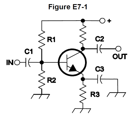
C2 removes the DC component from the output signal. If this is a power amplifier, the speaker or headphone is connected between the OUT terminal and ground. The current through the speaker is a fraction of that flowing through the un-numbered resistor and transistor.
Class B amplifiers are push-pull amplifiers, where each element conducts for less that 180 degrees. The 0.6 volt or similar drop means that there is a point at which the output drop from this voltage to 0 suddenly, then another delay before the negative device conducts at -0.6 volts. This therefore causes significant "cross-over distortion".
Class AB is a push-pull system which biases the devices such that each conducts for a little over 180 degrees (but clearly, much less than 360). This greatly reduces cross-over distortion.
Push-pull means that there is typically a complementary pair of devices, the NPN connected to the positive rail (say + 35 volts) and PNP to the negative rail (say -35 volts). The speaker is connected between the junction of the transistors, and ground. The voltage at the output is pushed and pulled by the two devices taking turns in conducting. The majority of the current passing through the transistors alsp passes through the speaker, making these much more efficient. These can also MOSFETs.
Class C is specifically for CW / Morse Code, where short pulses at the transmit frequency are fed into the tank circuit, which "fills in" the rest of the sine wave. The device conducts for much less than 180 degrees.
Class D uses a rapidly switching transistor or FET (often within an IC package), operating at many times the output frequency. They need an output filter network. These are somewhat similar to a switch-mode power supply. Most use is a audio frequencies, with some use on VLF.
You can see simplified diagrams here: Wikipedia: Power amplifier classes
This design requires only a fairly simple matching network to connect a 100 watt, 50 ohm HF transmitter as the input device. It feeds the cathode, with the output at the plate. See W8JI: Grounded Grid Amplifiers
These are the actual questions from the Extra licence exam pool, as published by the NCVEC.
E7A01
Which is a bi-stable circuit?
A. An AND gate
B. An OR gate
C. A flip-flop
D. A bipolar amplifier
Bi-stable means that the circuit has two stable states, and is also called a flip-flop, answer C.
E7A02
What is the function of a decade counter?
A. It produces one output pulse for every 10 input pulses
B. It decodes a decimal number for display on a seven segment LED display
C. It produces 10 output pulses for every input pulse
D. It decodes a binary number for display on a seven-segment LED display
This device generates a single output pulse for every 10 input pulses, answer A.
E7A03
Which of the following can divide the frequency of a pulse train by 2?
A. An XOR gate
B. A flip-flop
C. An OR gate
D. A multiplexer
A flip-flop, answer B.
E7A04
How many flip-flops are required to divide a signal frequency by 4?
A. 1
B. 2
C. 4
D. 8
If we divide by 2 twice we divide by 4, so 2 flip-flops are needed, answer B.
E7A05
Which of the following is a circuit that continuously alternates between two states without an external clock?
A. Monostable multivibrator
B. J-K flip-flop
C. T flip-flop
D. Astable multivibrator
Having no stable state, this is the astable multivibrator, answer D.
The 555 timer IC can be configured to do this, using just a few resistors and capacitors.
E7A06
What is a characteristic of a monostable multivibrator?
A. It switches momentarily to the opposite binary state and then returns to its original state after a set time
B. It produces a continuous square wave oscillating between 1 and 0
C. It stores one bit of data in either a 0 or 1 state
D. It maintains a constant output voltage, regardless of variations in the input voltage
From mono, meaning one, these have a single stable state. One of two possible behaviours is illustrated by this symbol: ⎍. Answer A.
E7A07
What logical operation does a NAND gate perform?
A. It produces logic 0 at its output only when all inputs are logic 0
B. It produces logic 1 at its output only when all inputs are logic 1
C. It produces logic 0 at its output if some but not all inputs are logic 1
D. It produces logic 0 at its output only when all inputs are logic 1
All inputs must be 1 (high) to produce a logic 0, answer D.
E7A08
What logical operation does an OR gate perform?
A. It produces logic 1 at its output if any or all inputs are logic 1
B. It produces logic 0 at its output if all inputs are logic 1
C. It only produces logic 0 at its output when all inputs are logic 1
D. It produces logic 1 at its output if all inputs are logic 0
If any or all inputs are high (1), a 1 will be produced, answer A.
E7A09
What logical operation is performed by an exclusive NOR gate?
A. It produces logic 0 at its output only if all inputs are logic 0
B. It produces logic 1 at its output only if all inputs are logic 1
C. It produces logic 0 at its output if only one input is logic 1
D. It produces logic 1 at its output if only one input is logic 1
As long as only a single input has a 1, a zero will be output, answer C.
E7A10
What is a truth table?
A. A table of logic symbols that indicate the high logic states of an op-amp
B. A diagram showing logic states when the digital device output is true
C. A list of inputs and corresponding outputs for a digital device
D. A table of logic symbols that indicate the logic states of an op-amp
A truth table lists the input states and corresponding output states, answer C.
E7A11
What type of logic defines "1" as a high voltage?
A. Reverse Logic
B. Assertive Logic
C. Negative logic
D. Positive Logic
This is standard "positive logic", answer D.
E7B01
For what portion of the signal cycle does each active element in a push-pull Class AB amplifier conduct?
A. More than 180 degrees but less than 360 degrees
B. Exactly 180 degrees
C. The entire cycle
D. Less than 180 degrees
This is a little over 180 degrees, answer A.
E7B02
What is a Class D amplifier?
A. A type of amplifier that uses switching technology to achieve high efficiency
B. A low power amplifier that uses a differential amplifier for improved linearity
C. An amplifier that uses drift-mode FETs for high efficiency
D. A frequency doubling amplifier
This is an amplifier which uses a high switching frequency to increase efficiency, answer A.
It may mean that a SM or DIP IC can produce several watts of audio without a heatsink, well beyond the power a similar sized linear device could without overheating.
E7B03
Which of the following components form the output of a class D amplifier circuit?
A. A low-pass filter to remove switching signal components
B. A high-pass filter to compensate for low gain at low frequencies
C. A matched load resistor to prevent damage by switching transients
D. A temperature compensating load resistor to improve linearity
As with D to A converters, a low pass filter is needed to remove switching components, answer A.
E7B04
Where on the load line of a Class A common emitter amplifier would bias normally be set?
A. Approximately half-way between saturation and cutoff
B. Where the load line intersects the voltage axis
C. At a point where the bias resistor equals the load resistor
D. At a point where the load line intersects the zero bias current curve
This is set half-way between saturation and cutoff, answer A.
E7B05
What can be done to prevent unwanted oscillations in an RF power amplifier?
A. Tune the stage for maximum SWR
B. Tune both the input and output for maximum power
C. Install parasitic suppressors and/or neutralize the stage
D. Use a phase inverter in the output filter
You can fit a resistor in parallel with coil or loop after the output device to provide parasitic suppression, and/or neutralise the stage, answer C.
E7B06
Which of the following amplifier types reduces or eliminates even order harmonics?
A. Push-push
B. Push-pull
C. Class C
D. Class AB
This is the push-pull amplifier, answer B.
E7B07
Which of the following is a likely result when a Class C amplifier is used to amplify a single-sideband phone signal?
A. Reduced intermodulation products
B. Increased overall intelligibility
C. Signal inversion
D. Signal distortion and excessive bandwidth
A Class C amplifier is quite simply the wrong device for SSB, and this will result in significant distortion, causing excessive bandwidth and thus interference, answer D.
E7B08
How can an RF power amplifier be neutralized?
A. By increasing the driving power
B. By reducing the driving power
C. By feeding a 180-degree out-of-phase portion of the output back to the input
D. By feeding an in-phase component of the output back to the input
Feeding an out-of-phase signal back into the input is called "negative feedback", and it neutralises the amplifier, answer C.
E7B09
Which of the following describes how the loading and tuning capacitors are to be adjusted when tuning a vacuum tube RF power amplifier that employs a Pi-network output circuit?
A. The loading capacitor is set to maximum capacitance and the tuning capacitor is adjusted for minimum allowable plate current
B. The tuning capacitor is set to maximum capacitance and the loading capacitor is adjusted for minimum plate permissible current
C. The loading capacitor is adjusted to minimum plate current while alternately adjusting the tuning capacitor for maximum allowable plate current
D. The tuning capacitor is adjusted for minimum plate current, and the loading capacitor is adjusted for maximum permissible plate current
The tuning capacitor is adjusted for minimum plate current, and the loading capacitor is adjusted for maximum permissible plate current, answer D.
E7B10
In Figure E7-1, what is the purpose of R1 and R2?
A. Load resistors
B. Voltage divider bias
C. Self bias
D. Feedback
This forms a voltage divider, to provide bias to the base, answer B.
E7B11
In Figure E7-1, what is the purpose of R3?
A. Fixed bias
B. Emitter bypass
C. Output load resistor
D. Self bias
R3 provides self bias, answer D.
E7B12
What type of amplifier circuit is shown in Figure E7-1?
A. Common base
B. Common collector
C. Common emitter
D. Emitter follower
This is a common emitter amplifier, as the emitter is essentially connected to ground, and both the input and output are referenced to ground, answer C.
E7B13
Which of the following describes an emitter follower (or common collector) amplifier?
A. A two-transistor amplifier with the emitters sharing a common bias resistor
B. A differential amplifier with both inputs fed to the emitter of the input transistor
C. An OR circuit with only one emitter used for output
D. An amplifier with a low impedance output that follows the base input voltage
This is a simple amplifier which has a high input impedance and a low output impedance, answer D.
It reproduces the input voltage at the output, but allows a signal with a high source impedance to drive a load with a low impedance.
E7B14
Why are switching amplifiers more efficient than linear amplifiers?
A. Switching amplifiers operate at higher voltages
B. The power transistor is at saturation or cut off most of the time, resulting in low power dissipation
C. Linear amplifiers have high gain resulting in higher harmonic content
D. Switching amplifiers use push-pull circuits
The output device switches rapidly between fully on and fully off, so there is little time when it is dissipating a large amount of power, answer B.
E7B15
What is one way to prevent thermal runaway in a bipolar transistor amplifier?
A. Neutralization
B. Select transistors with high beta
C. Use a resistor in series with the emitter
D. All of these choices are correct
A resistor in series with the emitter helps to stabilise the amplifier, answer C.
E7B16
What is the effect of intermodulation products in a linear power amplifier?
A. Transmission of spurious signals
B. Creation of parasitic oscillations
C. Low efficiency
D. All of these choices are correct
Intermodulation results in the transmission of spurious signals, answer A.
E7B17
Why are odd-order rather than even-order intermodulation distortion products of concern in linear power amplifiers?
A. Because they are relatively close in frequency to the desired signal
B. Because they are relatively far in frequency from the desired signal
C. Because they invert the sidebands causing distortion
D. Because they maintain the sidebands, thus causing multiple duplicate signals
These signals are close in frequency to the desired signal, answer A.
This means that the signals will generally be radiated efficiently by the associated antennas.
E7B18
What is a characteristic of a grounded-grid amplifier?
A. High power gain
B. High filament voltage
C. Low input impedance
D. Low bandwidth
This design of valve (tube) amplifier is low input impedance, answer C.
On to: Practical Circuits 2 - Filters & Power Supplies
You can find links to lots more on the Learning Material page.
Written by Julian Sortland, VK2YJS & AG6LE, June 2022.
Tip Jar: a Jefferson (US$2), A$3 or other amount / currency. Thanks!