Home - About AR - Learning Material - Exams - Clubs - Posters
The first practical transistors, like early diodes, used Germanium. These had the benefit of a low VBE, but had limitations in frequency handling and power handling, and could be easily damaged. For Australians, if you or your (grand) parents had an HMV record player or Radiogram in the late 1960s or early 1970s, then these used germanium transistors to drive 27 Ω speakers.
More modern devices use silicon. The VBE required for current to flow from base to emitter is 0.6 to 0.7 volts, and for an NPN is this is positive. This small base current allows a larger current to flow from the collector to the emitter.
Silicon is used in a range of additional devices, such as silicon control rectifiers (SCRs), Triacs, (both are called thyristors), UJTs, and FETs of many kinds; and of course, ICs.
Adding impurities to the semiconductor material forms P-type and N-type material.
Depending on the layering of the two material types, we can have NPN and PNP types. In days of old, PNPs were significantly less expensive, but now days they are equal. In audio power amplifiers a complementary pair is often used, with an NPN and PNP pair.
NPN transistors, mean the base is P-type, and the collector and emitter are N-type. These are often most useful for switching and small signal amplifiers when we have a supply which is positive with respect to ground, and these were used in both the circuit in the Technician paper, and later in this paper. In these devices, a current into the base, generated by a positive voltage on the base, allows a larger current to flow from the collector to the emitter.
One of the primary indicators of gain in a bipolar transistor is called beta, β. This is an indication of how much the collector current changes in response to a change in the base current. Note that for a particular part number there can be a wide range of gain figures, so if a device has a range from 25 to 100, you need to calculate for the lowest case. If you are using that transistor to switch a power LED or relay using 50 mA, you need to had a drive current of 2 mA, or better 2.5 mA. If we have 5 volts, subtract VBE, so 4.3 volts dropped across the resistor, R = E/I = 4.3 / 0.0025 = 1720 Ω. If we can't get an affordable 1720 ohm one, we can use try 1800 ohm one, I = E/R = 4.2 / 1800 = 002.333A, or 2.3333 mA, even if the supply voltage sags a little (you will see I put in a lower voltage), so a fine choice. Note that if the load is supplied by a higher voltage that is not a problem, provided it is within the specification of the transistor.
In such circuits the unnecessary base current cannot cause extra current to flow through the collector, as the load is the limiting factor. The problem would be if we built a batch of similar circuits, and set the base current to a level where for some devices the transistor did not turn on fully. In these cases there would be several volts between the collector and emitter, resulting in a high power dissipation, and possible failure of the device due to overheating.
Off the exam, an alternative term for beta, (β) is hfe meaning small signal AC gain; while hFE is DC gain, denoted as uppercase Beta (Β) in German papers. If you look at a list of transistors in a retail catalogue, you will see a range for each device listed under "HFE". There are a number of other "h-parameters".
Discussed later, due to the variation in gain, audio signal amplifiers are usually set up using a number of resistors to set the gain.
Off the exam, a "Darlington pair" consists of two transistors set up so that one transistor drives the second one, so that the first needs only a very small current, but requiring a higher voltage on the base. These are available in arrays, in DIL (IC-type) packages, such as the ULN2003AN.
Also not covered is the IGBT, the Insulated Gate Bipolar Transistor. These are used in industrial electronics, as they can switch large currents. For some of these FET-like devices, the gate voltage may need to exceed 5 volts.
Old transistor radios, and other circuits, were set up so they supply was negative in respect to common or ground, so PNPs could be used.
These are a little more like valves in their operation. An important parameter is their high input impedance. There are many kinds, including various junction FETS; and MOSFETS, with isolated gates.
The current carrying terminals are the Drain and Source, with control via the Gate.
Depletion mode FETs conduct current with no input on the gate, while a voltage on the gate acts as a noose, narrowing the channel, and reducing current flow.
Given there are many variations of FET, you may wish to read the Wikipedia article on FETs.
A power device with a low RDS, or resistance from Drain to Source means a low forward voltage drop, and low dissipation. It is possible to configure one to replace a diode to protect equipment from reverse power connection.
This a compound used to make transistors used in UHF, and especially microwave circuits. If you buy a VHF or UHF power amplifier, they may indicate that they include a GaAs-FET pre-amplifier. MMICs (microwave monolithic ICs), and some specialised logic ICs are also made using it.
Gunn Diodes, which generate microwaves, are made from GaAs.
The substance can also be used in space qualified solar cells, and IR LEDs.
Gallium Nitride, which we will discuss in a following page, is a newly exploited material, with lots of microwave and other applications.
Beyond simple rectifiers, there are many diodes with a range of special features, including for use in RF and microwave circuits.
These are a variation on the regular power rectifier diode, with a low forward voltage drop. This makes the maximum voltage available to the load, but also means the power wasted, and so needing to be dissipated in the diode is lower for a given current. P = I x VF, so the lower VF the better.
Remembering back to the Technician paper, these were used in a power supply as a simple voltage regulator.
The characteristic which make this work is that the voltage remains constant over a range of reverse currents. If the current is forwards the drop us around 0.6 volts, similar to a regular silicon diode.
While the most common use is as a shunt regulator, or as protection in case a power supply goes over-voltage, the other option is to use it as a voltage dropping component.
This simple circuit detects when a voltage is above about 19 volts, and is designed to indicate if a lighter outlet is supplying 24 volts (or 28 if the engine is running), rather than 12 volts. A 15 or 16 volt Zener is used, so unless the voltage is well above 14 volts, the LED won't light. If the voltage is 24 - 28 volts, then around 0.6 volt is dropped in the first diode (there in case the polarity is revered), 15 or 16 volts is dropped in the Zener, and 2 or 3 in the LEDs. The resistor is selected so the current is 20 mA with 28 volts on the circuit. The power is 16 v x 20 mA = 320 mW, so best to use a 1 watt, rather than 400 mW device if the device is to remain connected for any significant period.
When LEDs are forward biased, they emit visible, IR, or UV light. Most have a fairly narrow spectrum. Standard LEDs have a forward voltage drop of 1.8 to around 4 volts, depending on the material used, and therefore the colour. As an aside, old style yellowish green one drop about 2 volts, modern pure and bluish greens, around 3. In older papers IR LEDs are termed IREDs, infra-red emitting diodes, as used in remote controls, and now illumination for paranoia cameras...
Since around 2000 there have been high current blue LEDs with a yellow phosphor, which output what appears to be white light. These can replace incandescent lamps in many situations. These, and/or red versions can be used as light for field operations, perhaps two or 3 in series with a suitable power resistor, across 12 volts. 1 watt units typically use 300 mA; 3 watt ones, around 1 amp. These must be attached to a heatsink of some sort. There are also COB, with the die (chip) directly connected to the board, and the phosphor as a coating over the whole board.
These consist of P-type, undoped Intrinsic material, and N-type. These result in a large gap, and so low capacitance. They are thus useful as an RF switch or attenuator.
One question lists two interesting kinds of rectifiers as incorrect answers.
One is the Thermionic emission diode, alluding to diode valves or tubes. These were used as power rectifiers for various valve electronics, and included dual anode versions which were used as full-wave (not bridge) rectifiers.
Electrolytic rectifiers are rarely, if ever used now, but you can build one at home. They consist of a electrodes consisting of lead and aluminium (aluminum) in a solution of Sodium Carbonate (washing soda); and alum, meaning Potassium alum. Link. These concepts however led to the electrolytic capacitor.
While there are tricks to allow a FET with a low RDS in place of a series "idiot diode", to protect equipment for reverse polarity, with a lower forward drop, these are NOT diodes.
Off the exam, but interesting, are Selenium rectifier stacks. These have high forward voltage drops, so care needs to be taken if replacing these with modern devices, lest the supplied circuit be supplied with an excessive voltage. This also meant that power dissipation was high, so there they included large discs or squares of steel or aluminium for heatsinking, as well as acting as the substrate. The even earlier form of metal rectifier was the copper oxide rectifier. Mercury-arc and argon rectifiers are both plasma rectifiers. In the early 20th century NSW railways generated their own power at 25 Hz, and used mechanical rectification, using a synchronous motor and rotating contacts to convert it to DC for rail power.
Discharge of static electricity, especially through MOS / CMOS devices can blow a hole in the thin insulating silicon oxide layer, destroying the device, or damaging it so it fails later. This latent damage issue also applies to equipment which apparently survives a lightning strike.
While working with such equipment, it is wise to wear a static dispersing wrist-strap, and to work on a good quality static dissipative desk mat. These are grounded via a high value resistance (selected to if you do touch a mains voltage while wearing one the current through your body via the strap is limited to a safe level.
These are the actual questions from the Extra licence exam pool, as published by the NCVEC.
E6A01
In what application is gallium arsenide used as a semiconductor material in preference to germanium or silicon?
A. In high-current rectifier circuits
B. In high-power audio circuits
C. In microwave circuits
D. In very low frequency RF circuits
GaAs devices are used at microwave and UHF frequencies, answer C.
E6A02
Which of the following semiconductor materials contains excess free electrons?
A. N-type
B. P-type
C. Bipolar
D. Insulated gate
N type, N standing for negative has excess free electrons, remembering electrons are negatively charged, answer A.
E6A03
Why does a PN-junction diode not conduct current when reverse biased?
A. Only P-type semiconductor material can conduct current
B. Only N-type semiconductor material can conduct current
C. Holes in P-type material and electrons in the N-type material are separated by the applied voltage, widening the depletion region
D. Excess holes in P-type material combine with the electrons in N-type material, converting the entire diode into an insulator
The active parts of the P and N materials are separated by a widened depletion layer, answer C.
E6A04
What is the name given to an impurity atom that adds holes to a semiconductor crystal structure?
A. Insulator impurity
B. N-type impurity
C. Acceptor impurity
D. Donor impurity
Holes can accept current, so are the result of an acceptor impurity, answer C.
E6A05
How does DC input impedance at the gate of a field-effect transistor compare with the DC input impedance of a bipolar transistor?
A. They are both low impedance
B. An FET has lower input impedance
C. An FET has higher input impedance
D. They are both high impedance
FETs have significantly higher input impedance, answer C.
E6A06
What is the beta of a bipolar junction transistor?
A. The frequency at which the current gain is reduced to 1
B. The change in collector current with respect to base current
C. The breakdown voltage of the base to collector junction
D. The switching speed of the transistor
If 1 mA going into the base causes 100 mA to flow into the collector, then the beta (β) is 100, so answer B.
E6A07
Which of the following indicates that a silicon NPN junction transistor is biased on?
A. Base-to-emitter resistance of approximately 6 to 7 ohms
B. Base-to-emitter resistance of approximately 0.6 to 0.7 ohms
C. Base-to-emitter voltage of approximately 6 to 7 volts
D. Base-to-emitter voltage of approximately 0.6 to 0.7 volts
The key terms are silicon, meaning a voltage of 0.6 to 0.7 volts; and that the base to emitter junction is a PN junction, as indicated by the last two letters, so the voltage is positive between the base and emitter. Thus VBE is 0.6 to 0.7 volts, answer D.
E6A08
What term indicates the frequency at which the grounded-base current gain of a transistor has decreased to 0.7 of the gain obtainable at 1 kHz?
A. Corner frequency
B. Alpha rejection frequency
C. Beta cutoff frequency
D. Alpha cutoff frequency
This is the Alpha cutoff frequency, answer D.
RF amplifiers may ground the base, rather than use it as the input terminal in some RF circuits. Alpha is a way of comparing the change of collector current with respect to emitter current.
E6A09
What is a depletion-mode FET?
A. An FET that exhibits a current flow between source and drain when no gate voltage is applied
B. An FET that has no current flow between source and drain when no gate voltage is applied
C. Any FET without a channel
D. Any FET for which holes are the majority carriers
It is a FET which requires a voltage to constrict the current flow, answer A.
E6A10
In Figure E6-1, what is the schematic symbol for an N-channel dual-gate MOSFET?
A. 2
B. 4
C. 5
D. 6
In symbol 4, the isolation of the gates from the channel indicates it is a MOSFET, and the inward pointing arrow that the channel is made from N material, answer B.
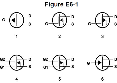
E6A11
In Figure E6-1, what is the schematic symbol for a P-channel junction FET?
A. 1
B. 2
C. 3
D. 6
In symbol 1, the connection of the gate to the channel indicates it is a junction FET, and the outward pointing arrow that the channel is made from P material, answer A.
E6A12
Why do many MOSFET devices have internally connected Zener diodes on the gates?
A. To provide a voltage reference for the correct amount of reverse-bias gate voltage
B. To protect the substrate from excessive voltages
C. To keep the gate voltage within specifications and prevent the device from overheating
D. To reduce the chance of static damage to the gate
The gate insulation is a thin layer, typically of silicon oxide. If you touch older MOSFETS or older CMOS ICs without using static protection, there is every chance you will damage the device, due to static discharge from your body to the device, blowing a tiny hole in this insulation layer, answer D.
The Zener diode(s) can generally dissipate this energy safely. Note that you may build a PC without wearing a wrist-strap, and it works fine now, but may well fail in a few months.
E6B01
What is the most useful characteristic of a Zener diode?
A. A constant current drop under conditions of varying voltage
B. A constant voltage drop under conditions of varying current
C. A negative resistance region
D. An internal capacitance that varies with the applied voltage
As the current through the device varies, the voltage stays constant, answer B.
E6B02
What is an important characteristic of a Schottky diode as compared to an ordinary silicon diode when used as a power supply rectifier?
A. Much higher reverse voltage breakdown
B. More constant reverse avalanche voltage
C. Longer carrier retention time
D. Less forward voltage drop
These have a lower forward voltage drop, and so lower power dissipation, answer D.
E6B03
What type of bias is required for an LED to emit light?
A. Reverse bias
B. Forward bias
C. Zero bias
D. Inductive bias
Current must pass forward through an LED for it to emit light, so answer B, forward bias.
E6B04
What type of semiconductor device is designed for use as a voltage-controlled capacitor?
A. Varactor diode
B. Tunnel diode
C. Silicon-controlled rectifier
D. Zener diode
Varying the negative bias on a varactor diode effectively varies the distance between the plates of the capacitor formed by the diode elements in their non-conducting state. Bog standard diodes also exhibit this effect to some degree, but varactors are designed to maximise it, answer A.
If you had a VHS or maybe a Beta machine with small multi-turn adjustable resistors (trim-pots) to set each channel, then I expect these were selectively connected to a varactor in the tuner, to select the TV channel to watch or record.
E6B05
What characteristic of a PIN diode makes it useful as an RF switch?
A. Extremely high reverse breakdown voltage
B. Ability to dissipate large amounts of power
C. Reverse bias controls its forward voltage drop
D. Low junction capacitance
The large band of undoped or intrinsic material, means it has low capacitance, answer D.
E6B06
Which of the following is a common use of a Schottky diode?
A. As a rectifier in high current power supplies
B. As a variable capacitance in an automatic frequency control circuit
C. As a constant voltage reference in a power supply
D. As a VHF/UHF mixer or detector
These are used at VHF and UHF as a mixer or detector, answer D
These are also termed Hot carrier diodes, and use can extend into the microwave range.
E6B07
What is the failure mechanism when a junction diode fails due to excessive current?
A. Excessive inverse voltage
B. Excessive junction temperature
C. Insufficient forward voltage
D. Charge carrier depletion
As with a resistive component, or even a wire, excessive current causes excessive heating of the diode's junction, leading to failure, answer B.
Standard power diodes can survive brief pulses much greater than their rated current, but if an excessive current is maintained for a period, they will fail.
E6B08
Which of the following is a Schottky barrier diode?
A. Metal-semiconductor junction
B. Electrolytic rectifier
C. CMOS-field effect
D. Thermionic emission diode
This is a metal to semiconductor junction, answer A.
E6B09
What is a common use for point-contact diodes?
A. As a constant current source
B. As a constant voltage source
C. As an RF detector
D. As a high-voltage rectifier
These are used as an RF detector, including in modern "crystal sets", a basic AM receiver, answer C.
E6B10
In Figure E6-2, what is the schematic symbol for a light-emitting diode?
A. 1
B. 5
C. 6
D. 7
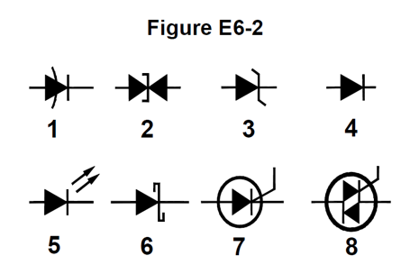
The arrows in symbol 5 indicates it is emitting light, answer B.
E6B11
What is used to control the attenuation of RF signals by a PIN diode?
A. Forward DC bias current
B. A sub-harmonic pump signal
C. Reverse voltage larger than the RF signal
D. Capacitance of an RF coupling capacitor
This is forward DC current, answer A.
On to: Components 2 - Logic ICs, PLDs, Inductors, & Piezoelectric devices
You can find links to lots more on the Learning Material page.
Written by Julian Sortland, VK2YJS & AG6LE, June 2022.
Tip Jar: a Jefferson (US$2), A$3 or other amount / currency. Thanks!