Home - About AR - Learning Material - Exams - Clubs - Posters
While early logic was RTL, then DTL (resistor-transistor logic, then diode-transistor logic); this has mostly gone by the wayside, TTL, or transistor-transistor logic remains a fairly common form of logic. This uses bipolar transistors. The supply must be 5 volts, and current consumption tends to be high. It can operate at high speed, especially the F versions. NPN transistors are used within the ICs, and in most cases outputs are pulled high or low by operating one or other of the two output transistors.
Off the exam, the part numbers commence with 74 for consumer grade, and 54 for Mil-spec (military specification).
That said, you can still use 1N4148 diodes and/or NPN transistors to perform logic functions.
CMOS, standing for Complementary metal‐oxide‐semiconductor, is the newer family, with low current consumption. It is so named because it uses complementary and symmetrical pairs of p-type and n-type MOSFETs. The output(s) are actively pulled towards the rails by one or other of the two types of MOSFETS.
Also off the exam, part numbers start with 40 or 45. 74 series with a C in the letter(s) following the 74 are also CMOS.
In most cases, including TTL and CMOS, low (Logic 0) means near the negative or ground rail, and high (Logic 1) means near the positive supply rail. For TTL this is 0 and +5 volts. Certainly in older equipment logic can be inverted, or can operate using negative voltages. An example is the double refrigerator sized IBM 608 calculator (their first all transistor unit) from 1957 appears to have used 0 and -5 volts, with rails at +5. 0, -5, and -10 volts for the diode-transistor logic. It primarily processed data stored on punched cards.
The question which sought the benefit of "low power consumption" for CMOS logic has been replaced by one asking for the family with the lowest consumption, which again is CMOS.
Off the exam, but perhaps useful as background, NMOS and PMOS were used in early processors and associated ICs, and are named for the n-type or p-type MOSFETs used.
NMOS was a family from the era of the VIC-20 home computer, with high power consumption to the point that heating of the IC caused low reliability in the 6502 processor and Video Interface Chip. They also had undocumented operations not present in the later CMOS versions. Like a discrete transistor inverter the output is pulled high by a resistor, but in this case internal. As an example an NMOS NOR gate uses essentially parallel MOSFETs to pull the output low when one or both inputs are high (illustrated in the article linked to below). Thus current flows in the pull-up resistor whenever the output is low, causing heating within the IC, which can be multiplied many times if there are many gates.
PMOS is another mostly discontinued family, needing 17 to 24 volts, although there was as trick with the Intel 4004 processor, where +5 and -10 volt rails were used to allow it to work with TTL.
You can read the following Wikipedia articles if you wish: TTL, CMOS, NMOS, Depletion Load NMOS & HMOS, and PMOS. Fairchild's application note AN-77 on CMOS is interesting too.
Another upside of CMOS vs NMOS or PMOS is that they can drive very small loads, such as LEDs via a resistor which limits the current to a few mA via sourcing OR sinking. Sourcing means current flows from a high output to ground; sinking from a LED and resistor connected to the positive rail, to a low output. TTL can source a few mA and source around 10 mA. Specialised ICs, such as Nixie tube drivers, can sink current from a device connected to 50 or more volts.
Another is ECL, emitter coupled logic, which can use differential signalling. It was the fabled family when I was younger, for its very high speed, but standard ECL needs -5.2 volts to operate, with Low being -1.75 V, and High -0.9 V. It is power hungry. Wiki: ECL
There is an industry working group called "Beyond CMOS", looking at future options without some of the limits of CMOS. Others are looking at device packaging, manufacturing, measurement, improved yield (many ICs within a wafer may fail, or pethaps be sorted from a premium op-amp part number bin to the μA741 bin), and more.
Below are five logic gates (using ANSI symbols), as well as an older operational amplifier symbol, as a distractor, at 6.
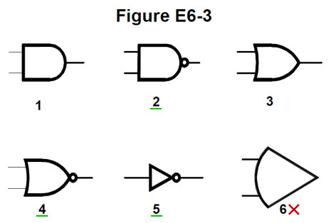
At item 5 is the inverter or NOT gate. Important and "important", this device has a single input, and outputs the opposite level, 1 becomes 0, 0 becomes 1. The circle on its output indicates this function. Without the ring, buffers are also available, and are used to distribute a signal around a board to many inputs, or perhaps to drive a small load, such as an LED. Yes, a buffer and the block diagram symbol for an amplifier have the same symbol. Two inverters can be used to make a buffer.
The ring can also appear at inputs, meaning that it is "active low", such as a reset pin, often marked RESET with the overbar also indicating it is inverted. Thus the pin us pulled to ground to reset a processor or counter. A common trick is to place a capacitor to ground on this pin, with a resistor to charge it. This ensures the IC is in the base condition after power up.
1 and 2 are the AND and NAND gates. The output of an AND gate is high only when both inputs are high. The circle on the NAND indicates the output is inverted, meaning is high unless both inputs are high. These have a straight line at the input, and a semi-circle at the output.
3 and 4 are OR and NOR gates. And OR gate has a high output if one or both inputs are high. A NOR gate is high unless one or both of the inputs are high. The concave curve at the input side, and Gothic arch at the output are the features to note.
Off the exam, exclusive-OR or X-OR gates are high only when one, but not both, inputs are high. X-NOR have an inverted output compared to this. These have a the same curve at the input repeated to the left of the input.
These are covered again on Practical Circuits 1 - Digital circuits & Amplifiers, where I have included Truth Tables. (This link should open in a new tab, which you can close when finished).
While tiny surface mount packages are available which hold a single gate, in most cases they are in a 14 pin DIL / DIP / PDIP packages. These have 2 pins for power, and 12 for logic, allowing 6 inverters or buffers; or four 2-input gates, three 3-input gates, two 4-input, or single 8-input gates. Hex, Quad, Triple, and Double are often used in the description. ICs with a combination of different gates are or were available, some in 16 pin packages.
There are various further counters, flip-flops, latches, adders, etc, some in 24 pin or larger cases.
The 40107 is an 8 pin IC with two NAND gates with an "open drain" output, meaning it is useful for driving an LED or relay, as long as two conditions are met.
Operational amplifiers (Op-amps) at 6 are discussed on a subsequent page. The convex curve on the input side appears to be a US specific thing, and even then deprecated, except in ARRL publications. These are not as out of place as you may think, as they can be formed into analogue computers.
Some ICs and other circuits may have an open collector output, where a zero is indicated by the line being pulled to ground, but left open for 1. Thus a resistor to the connected from the input of the following device to the positive rail. 10 kΩ is typical.
If using signal diodes as an OR gate, a 1 will be asserted by the input to the diode(s), but a resistor is needed to ensure the input is pulled to ground when there in no high feeding the diodes.
This also applies when switches are used as inputs, in some cases when taking a signal from an external device. The active low RESET input above may also be operated by having a resistor to the positive rail, and a normally-open push-button positioned so a ball-point pen or opened out paper-clip is needed to push it.
Beyond the exam, inputs to unused gates should be tied to ground or supply, generally directly. Unused inputs on a multi-input gate should be tied low on an OR, high on an AND.
More modern is BiCMOS. This allows elements which benefit from being CMOS, such as the high impedance (FET) inputs using this technology; while elements needing high speed, and especially low impedance, such as the outputs using bipolar transistors, as TTL does. BiCMOS is also used in Op-Amps, while SiGeC (Silicon-Germanium-Carbon) BiCMOS is in some cases replacing GaAs in RF circuitry.
In many computerised system, there are data buses of multiple lines (say 8 or 16 bits wide). At various times the processor and other devices take turns in reading and writing data along the bus. Thus devices have to be able to both assert a 1 or 0; or to remain in a high impedance state while other devices communicate.
This is also used in many micro-controller ICs and single board computers, where a pin can be switched between being an input, or an output.
This is an IC which compares the voltage of 2 inputs, and switches the output between its two rails depending on the values on the inputs. A typical unit may put the output high if the +ve input exceed the -ve one, and low if it does not. There is normally some hysteresis to prevent noise on a signal close to the reference voltage from causing the unit to switch rapidly between states.
You can use them to indicate the state of a battery. It is common to use voltage dividers to "condition" the sampled voltage to the range of the device, as generally the input to the IC pins should be between the supply rails. Check with the data sheet.
The Voltage divider rule is: Vout = Vin × (R2 / R1+R2)
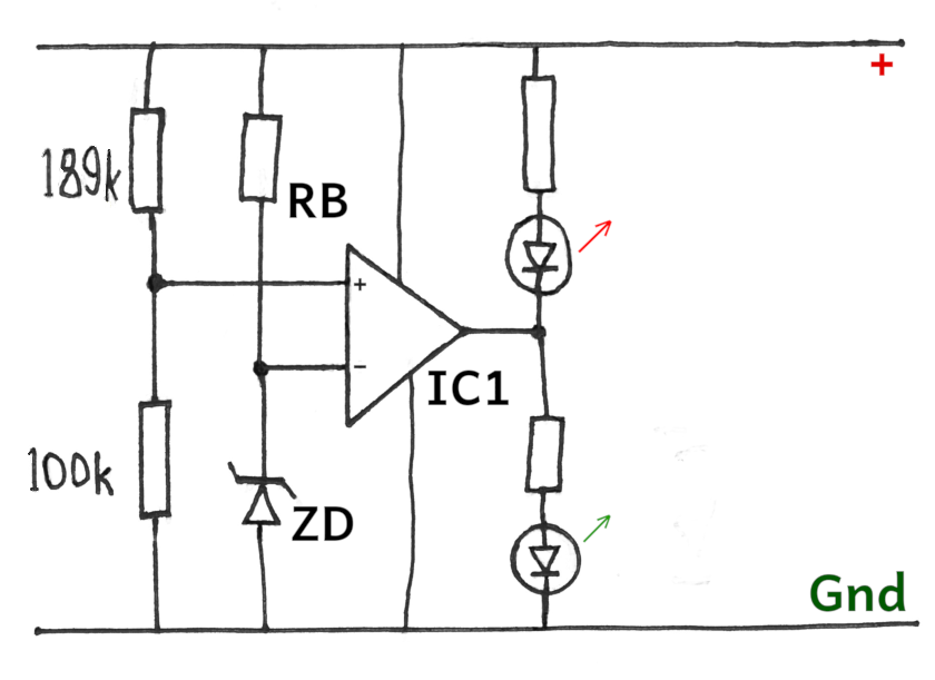
| This is a comparator circuit which compares the voltage of the supply rail with the value of a zener diode. The two resistors for a voltage divider so that sample on the positive input is 100 / 289 = 0.346 of the supply voltage. RB biases zener diode. If the sample voltage exceeds the zener voltage then the output will be high and the lower (green) LED lit. If it is lower, say due to a low battery then the output is low, and the upper (red) LED glows. 4.15 volt zeners are available at professional suppliers in surface mount (ditto the 189 ohm and close tolerance 100 ohm resistors). This gives a transition voltage of 4.15 / 0.349 = 11.994 volts. High street through-hole 4.1 volt devices give: 4.1 / 0.349 = 11.85 volts. |
Read the comparator's current sourcing and sinking specification, but the LED resistors should be several kilohms to keep the current through the device sensible. Or drive the base of a transistor (or Darlington) to operate the LED, and an inverter (transistor or IC) to drive a second transistor for the other LED. (Or maybe you cna use a PNP for the second LED, which becomes active when the output is low). Rz could be (12-4.15) / 0.005 = 7.85 / 0.005 = 1570 ohms. 1.5 kΩ is fine. Multiplying this out for 16 volts on the input gives 8 mA and just under 35 mW on the Zener, and under 100 mW on the resistor. There are also a range of other voltage standard diode and 2 or 3 pin ICs with closer tolerance.
You could also use a 180 kΩ and a 100 kΩ resistor, but make the junction of the divider and the + input a 50 kΩ multi-turn trimpot, using a high street 4.1 or 4.3 volt zener, and set the transition point against a variable supply and a multimeter.
LM311 is a famous example, and LP311 its low power cousin. LM393 is a dual device, which would allow an over and under voltage indicator. Note that some may have open collector outputs instead of driving the output to both rails. Op-amps can be used in their place in some cases. The 555 timer uses a couple internally, with the reference points set by the internal chain of 5 kΩ resistors.
Field-programmable gate array (FPGA) are advanced ICs which can now contain at least 50 million gates. They are a development on PLAs, PALs, and GALs which allowed companies to replace a PCB full of logic gates with a single customisable or programmable chip. Modern ones can include DSP, processor, and IP data communication as "hard blocks", or processors can be added as "soft blocks". "Important" to note is that they are programmed using "Hardware description language (HDL)".
Going further, these can be used to build a form of software defined radio. You can likley build things such as open source "CODEC2" voice codecs, as well as DMR and similar codecs, although in the latter case it may be best to stay anonymous, as the people which make huge amounts from the codec ICs get all whiney about open source alternatives. There is no reason a radio's processor cannot also perform the codec functions, except for "rights" / greed issues. The FPGA could also drive the display, read button presses, etc.
Certain materials, when an electric current is applied, deform. This is used in devices such as some tweeters (high frequency speakers), beepers, noise-making toys, ultrasonic cleaners, and ultrasonic anti-fouling transducers for boats. In some cases these are driven with voltages above 100 volts, potentially made more hazardous by the presence of salty water.
Such materials also convert force into electricity and so can be can be used as vibration or impact sensors, certain microphones, energy recovery, vandal resistant switches (Sydney folk will see these in emergency help points on railway stations), the spark generator in some cookers and electric cancer-stick lighters, and devices with claim to alleviate mosquito bite pain using an electric pulse.
Piezo is a transliteration of the Greek πιέζω, meaning to squeeze in ancient language, or to press in the modern one. Further meanings are to repress or stifle (ancient), and figuratively to be stressed (modern).
Transliteration is the display of a word from a language which uses a different script, such as Hebrew or Persian, in our "Latin" or "Roman" script (or the opposite). The name of the radio company "Yaesu Musen" transliterates the name of the Tokyo district the company was established in, and the word "wireless"; using a system called "Romaji". Cyrillisation allows a Ukrainian to order суші (sushi). Pinyin is the common system to transliterate Chinese.
Crystals, typically consisting of a slice of quartz crystal, also use the Piezoelectric effect. These set the frequency of channels in older two-way radios, but also the master oscillator in modern radios, and for all manner of processors. Much modern technology would have been very difficult to create without them, including NTSC or PAL colour TV. Quartz is silica (silicon dioxide).
The equivalent circuit of such a crystal consists of "Series RLC in parallel with a shunt C representing electrode and stray capacitance". These are illustrated in the diagram below.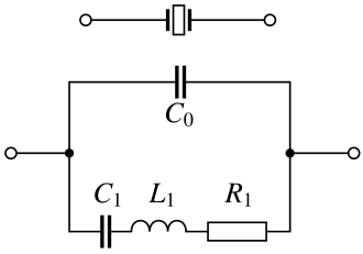
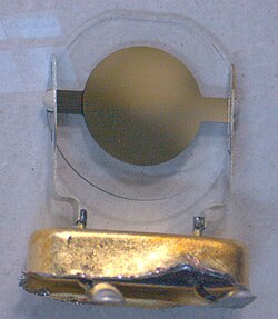
You can see the similarity between the crystal and capacitor symbols (left / top), and the capacitor-like metalisation forming the connection on a disc of clear crystal material (right / lower). It is from an HC-49/U sized package, and likely around 9 mm wide overall. This size is available with solderable wire leads; or thicker pins, allowing CB or remote contral channels to be swapped. There were various larger cases, and now smaller packages, including surface mount.
The previous version of the answer was more extensive: "Motional capacitance, motional inductance, and loss resistance in series, all in parallel with a shunt capacitor representing electrode and stray capacitance".
You can read more on Wikipedia: Crystal oscillator, especially the "Electrical model" setion; and even more on the IEEE's Frequency Control pages, archived on the Wayback Machine: IEEE UFFC: Introduction to Quartz Frequency Standards.
If you go to a gemstone or New Age / hippy shop, or a seller at a fair, you can see quartz as pieces of what looks like translucent glass in a hexagonal shape, like a few centimetres of pencil, but with a less acute angle at the point. AliExpress sellers have clusters. Other forms and colours exist. Being silica, breathing powder or dust is harmful, but a simple display item should be safe. The idea that sticking one to a CRT monitor to block radiation is complete "woo".
From near DC to gigahertz, inductors and transformers are vital in radio systems.
At mains and audio frequencies the use of laminated steel is common. Laminations typically consist of steel with a "blue" oxide layer. This layer insulates the laminations from each other elecrtrically, while still allowing the magnetic circuit to exist. While visible on many EI and C-core transformers, toroid power transformers also use laminations.
At RF frequencies ferrite (a ceramic made from Manganese-zinc and iron oxide, or Nickel-zinc and iron oxide); or iron powder cores are used. The examiner wants you to know that fewer turns may be needed for a particular inductance on ferrite than iron powder. The core material property which determines inductance is Permeability, the longer of the two similar words offered. Its symbol is μ, and it is the inverse of reluctance.
Inserting brass (a corrosion resistant copper alloy used for screws and bolts) reduces inductance.
Air-cored inductors are also an option.
These are the actual questions from the Extra licence exam pool, as published by the NCVEC.
E6C01
What is the function of hysteresis in a comparator?
A. To prevent input noise from causing unstable output signals
B. To allow the comparator to be used with AC input signal
C. To cause the output to change states continually
D. To increase the sensitivity
This prevents noise causing the input from fluttering between low and high outputs, answer A.
E6C02
What happens when the level of a comparator's input signal crosses the threshold?
A. The IC input can be damaged
B. The comparator changes its output state
C. The reference level appears at the output
D. The feedback loop becomes unstable
When the input changes to a voltage above or below the reference input, the output will change state, answer B.
E6C03
What is tri-state logic?
A. Logic devices with 0, 1, and high impedance output states
B. Logic devices that utilize ternary math
C. Logic with three output impedances which can be selected to better match the load impedance
D. A counter with eight states
This is binary logic, with the usual 0 and 1 outputs, plus the ability to not assert a value on the bus, answer A.
Micro-controller ICs often do this, and can use the same pin as an input.
E6C04
Which of the following is an advantage of BiCMOS logic?
A. Its simplicity results in much less expensive devices than standard CMOS
B. It is immune to electrostatic damage
C. It has the high input impedance of CMOS and the low output impedance of bipolar transistors
D. All these choices are correct
BiCMOS has the high input impedance of a CMOS (FET) input, and the low output impedance of bipolar transistors, answer C.
E6C05
Which of the following digital logic families has the lowest power consumption?
A. Schottky TTL
B. ECL
C. NMOS
D. CMOS
NMOS has low power consumption, and are more suitable for battery powered circuits, answer D.
E6C06
Why do CMOS digital integrated circuits have high immunity to noise on the input signal or power supply?
A. Large bypass capacitance is inherent
B. The input switching threshold is about two times the power supply voltage
C. The input switching threshold is about half the power supply voltage
D. Bandwidth is very limited
To go from 0 to 1, the input must exceed half the supply voltage, or from 1 to 0, below half the supply, answer C.
In most cases the inputs are fairly close to the ground or positive rail, so it would take a great deal of noise the cause the input to the wrong state.
E6C07
What best describes a pull-up or pull-down resistor?
A. A resistor in a keying circuit used to reduce key clicks
B. A resistor connected to the positive or negative supply line used to establish a voltage when an input or output is an open circuit
C. A resistor that ensures that an oscillator frequency does not drive lower over time
D. A resistor connected to an op-amp output that prevents signals from exceeding the power supply voltage
This is a resistor to set a level when the input would otherwise be open, say down to ground when the input is an SPDT switch contact to the positive rail; or to pull it up when the input is an open collector output, which goes to ground when the input is active, answer B.
E6C08
In Figure E6-3, what is the schematic symbol for a NAND gate?
A. 1
B. 2
C. 3
D. 4
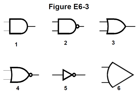
The flat input end, and semi-circular output end means AND, but we want a NAND, with the output inverted, so we need the one with the circle on the output, item 2, answer B.
E6C09
What is used to design the configuration of a field-programmable gate array (FPGA)?
A. Karnaugh maps
B. Hardware description language (HDL)
C. An auto-router
D. Machine and assembly language
These consist of a very large number of logic gates and circuits in a single IC, which can be programmed into complex logic systems using hardware description language, answer B.
These can be faster than processors for some tasks. All distractors are real things, the first relating to boolean algebra (logic). The others relate to placing PCB tracks using CAD, and more efficient programming of early processors and microcontrollers.
E6C10
In Figure E6-3, what is the schematic symbol for a NOR gate?
A. 1
B. 2
C. 3
D. 4
The OR function is indicated by the curved input, and the Gothic arch turned sideways. This is converted to NOR bu the the circle on the output, as in item 4, answer D.
Gothic arches are seen in many traditional church buildings, and some historic public or university buildings, including above doors and windows.
E6C11
In Figure E6-3, what is the schematic symbol for the NOT operation (inversion)?
A. 2
B. 4
C. 5
D. 6
These have a single input and a single output, with an inversion circle on output, item 5, answer C.
E6D01
What is piezoelectricity?
A. The ability of materials to generate electromagnetic waves of a certain frequency when voltage is applied
B. A characteristic of materials that have an index of refraction which depends on the polarization of the electromagnetic wave passing through it
C. A characteristic of materials that generate a voltage when stressed and that flex when a voltage is applied
D. The ability of materials to generate voltage when an electromagnetic wave of a certain frequency is applied
Deforming a piece of piezoelectric material generates a pulse of electricity, while applying power deforms them, answer A.
E6D02
What is the equivalent circuit of a quartz crystal?
A. Series RLC in parallel with a shunt C representing electrode and stray capacitance
B. Parallel RLC, where C is the parallel combination of resonance capacitance of the crystal and electrode and stray capacitance
C. Series RLC, where C is the parallel combination of resonance capacitance of the crystal and electrode and stray capacitance
D. Parallel RLC, where C is the series combination of resonance capacitance of the crystal and electrode and stray capacitance
This is series RLC in parallel with a shunt C representing electrodes, and stray capacitance, such as to the case, answer A.
Yikes, lots of similar answers. but it is a somewhat complex arrangement. Importantly, it is the shortest answer.
E6D03
Which of the following is an aspect of the piezoelectric effect?
A. Mechanical deformation of material by the application of a voltage
B. Mechanical deformation of material by the application of a magnetic field
C. Generation of electrical energy in the presence of light
D. Increased conductivity in the presence of light
The piezoelectric effect is used in some truck reversing bleepers, alarms etc, and are available as either complete beepers with the oscillator and driver; or as just the element, with or without an enclosure. In either case, the material is coated onto a thin metal disc. So, yes, the voltage applied deforms the material, answer A.
E6D04
Why are cores of inductors and transformers sometimes constructed of thin layers?
A. To simplify assembly during manufacturing
B. To reduce power loss from eddy currents in the core
C. To increase the cutoff frequency by reducing capacitance
D. To save cost by reducing the amount of magnetic material
As far as mains frequency inductors and power transformers go, laminated steel is used by default, as these reduce loss from eddy currents in the core, answer B.
E6D05
How do ferrite and powdered iron compare for use in an inductor core?
A. Ferrite cores generally have lower initial permeability
B. Ferrite cores generally have better temperature stability
C. Ferrite cores generally require fewer turns to produce a given inductance value
D. Ferrite cores are easier to use with surface-mount technology
Fewer turns are generally required for a certain inductance, answer C.
E6D06
What core material property determines the inductance of an inductor?
A. Permittivity
B. Resistance
C. Reactivity
D. Permeability
The only answer which relates to magnetism is permeability, answer D.
The first on relates to capacitors.
E6D07 - Withdrawn!
It was realised that both "excitation current" and "magnetising current" flow in the primary of an unloaded transformer, meaning two options were correct.
E6D08
Which of the following materials has the highest temperature stability of its magnetic characteristics?
A. Brass
B. Powdered iron
C. Ferrite
D. Aluminum
This is iron powder, answer B.
These can handle larger currents. The chirpy 28 MHz power oscillator based CW transmitter I built uses an iron-powder toroidal core as its output transformer, despite the author listing it as ferrite core.
E6D09
What devices are commonly used as VHF and UHF parasitic suppressors at the input and output terminals of a transistor HF amplifier?
A. Electrolytic capacitors
B. Butterworth filters
C. Ferrite beads
D. Steel-core toroids
Ferrite beads increase the inductance of the conductors, but the reactance at HF is much lower than at VHF or UHF, so VHF and UHF signals are attenuated (filtered), while HF ones pass, answer C.
E6D10
What is a primary advantage of using a toroidal core instead of a solenoidal core in an inductor?
A. Toroidal cores confine most of the magnetic field within the core material
B. Toroidal cores make it easier to couple the magnetic energy into other components
C. Toroidal cores exhibit greater hysteresis
D. Toroidal cores have lower Q characteristics
The majority of the magnetic energy is contained within the core, answer A.
E6D11
Which type of core material decreases inductance when inserted into a coil?
A. Ceramic
B. Brass
C. Ferrite
D. Aluminum
Inserting brass (a copper alloy) into a coil reduces its inductance, answer B.
E6D12
What causes inductor saturation?
A. Operation at too high a frequency
B. Selecting a core with low permeability
C. Operation at excessive magnetic flux
D. Selecting a core with excessive permittivity
Saturation happens when operating an inductor at excessive magnetic flux, answer C.
Another way to express this is that the ability of the inductor's core to store magnetic energy has been exceeded.
Way off the exam, European diagrams may replace the logic symbols with blocks containing symbols, as per the IEC standard: & is AND. ≥1 for OR, as the values must be 1 or greater. =1 is an XOR gate, as there must be a value of exactly 1 for it to set the output high.
To invert the output these symbols had a small slash \ linking the block and the output.
More a thought exercise than a gate you can buy, another pair of gates are IMPLY and NIMPLY. IMPLY has the output high unless A is 1 and B is 0, that is, A is greater that B. NIMPLY reverses the output. Its ANSI symbol has a inversion circle on the A input of an OR (or NOR) gate. The IEC symbols contain =B. You could build them using other gates. I had a car radio which included a DVD player. It only played DVD video to the tiny front panel screen if the Accessories line was high but the ignition was low. I think that is NIMPLY. They are mostly used in logic associated wth genetics.
Visit: Wikipedia: Logic gate for symbols in both styles. The article for each gate includes the internal or discrete diagram for each gate, and the DIN symbol, which uses semi-circles.
One deleted question looped back to a past topic. The primary cause of inductor self-resonance is: Inter-turn capacitance. Turns in an inductor often consist of copper windings separated only by a thin layer of enamel insulation. Metal layers, separated by thin layers of insulation, we call that a capacitor! Yes, it is the inter-turn capacitance.
Another asked why should core saturation of an impedance matching transformer be avoided? This is because harmonics and distortion could result.
On to: Components 3 - Analogue ICs & Optoelectronics
You can find links to lots more on the Learning Material page.
Written by Julian Sortland, VK2YJS & AG6LE, December 2025.
Tip Jar: a Jefferson (US$2), A$3 or other amount / currency. Thanks!
You can also buy me a non-coffee beverage: ko-fi.com/ag6le