Home - About AR - Learning Material - Exams - Clubs - Posters
The first practical transistors, like early diodes, used Germanium. These had the benefit of a low VBE, but had limitations in frequency handling and power handling, and could be easily damaged. For Australians, if you or your (grand) parents had an HMV record player or Radiogram in the late 1960s or early 1970s, then these used germanium transistors to drive 27 Ω speakers.
Using the European Pro Electron system, AC and AD are signal and power germanium transistors for audio frequencies. AF is for RF. OC was also used, meaning a triode with no heater.
More modern devices use silicon. The VBE required for current to flow from base to emitter is 0.6 to 0.7 volts, and for an NPN is this is positive. This small base current allows a larger current to flow from the collector to the emitter.
BC and BD are signal and power audio frequency silicon transistors. BF is for RF, BU for switching DC current. 2N is the US system, and 2S is used in Japan. MRF is used on Motorola RF power devices, used in the final stage of various transceivers.
Silicon is used in a range of additional devices, such as IGBTs, UJTs, and FETs of many kinds; and of course, ICs. There are a wide range of thyristors such as silicon control rectifiers (SCRs), GTOs, DIACs, and Triacs, ranging in size from a domestic light dimmer to industrial use, to grid scale, an example being high stacks rated at 1800 Amps and 275 kV for HV DC power transmission. The latter uses very large numbers modules in series, each consisting of say 6 hockey puck units in parallel. LASCRs, Light Activated SCRs, could be used in trigger additional flash units for photography, although they are apparently no longer made.
Alternative materials are used in modern high performance devices, discussed below.
Adding impurities to the semiconductor material forms P-type and N-type material.
Depending on the layering of the two material types, we can have NPN and PNP types. In days of old, PNPs were significantly less expensive, but now days they are equal. In audio power amplifiers a complementary pair is often used, with an NPN and PNP pair.
In NPN transistors the base is P-type, and the collector and emitter are N-type. These are often used for switching and small signal amplifiers when we have a supply which is positive with respect to ground, and these were used in both the circuit in the Technician paper, and later in this paper. In these devices, a current into the base, generated by a positive voltage on the base, allows a larger current to flow from the collector to the emitter.
Common dopants for n type are phosphorus and arsenic, with free electrons, also termed a donor impurity. Boron is an example of p-type, causing "holes", also termed an acceptor impurity. See: Wikipedia: Doping. Phosphorus can be added chemically, or by exposing silicon to a neutron stream from a research sized nuclear reactor, causing it to transmute!
One of the primary indicators of gain in a bipolar transistor is called beta, β. This is an indication of how much the collector current changes in response to a change in the base current. Note that for a particular part number there can be a wide range of gain figures, so if a device has a range from 25 to 100, you need to calculate for the lowest case. If you are using that transistor to switch a power LED or relay using 50 mA, you need to had a drive current of 2 mA, or better 2.5 mA. If we have 5 volts, subtract VBE, so 4.3 volts dropped across the resistor, R = E/I = 4.3 / 0.0025 = 1720 Ω. If we can't get an affordable 1720 ohm one, we can use try 1800 ohm one, I = E/R = 4.2 / 1800 = 0.002333 A, or 2.3333 mA, even if the supply voltage sags a little (you will see I put in a lower voltage), so a fine choice. Note that if the load is supplied by a higher voltage that is not a problem, provided it is within the specification of the transistor.
In such circuits the unnecessary base current cannot cause extra current to flow through the collector, as the load is the limiting factor. The problem would be if we built a batch of similar circuits, and set the base current to a level where for some devices the transistor did not turn on fully. In these cases there would be several volts between the collector and emitter, resulting in a high power dissipation, and possible failure of the device due to overheating.
Off the exam, an alternative term for beta, (β) is hfe meaning small signal AC gain; while hFE is DC gain, denoted as uppercase Beta (Β) in German papers. If you look at a list of transistors in a retail catalogue, you will see a range for each device listed under "HFE". There are a number of other "h-parameters". (This is not ß, replacing ss or sz).
Discussed later, due to the variation in gain of transistors, audio signal amplifiers are usually set up using a number of resistors to set the gain.
Off the exam, a "Darlington pair" consists of two transistors set up so that one transistor drives the second one, so that the first needs only a very small current, but requiring a higher voltage on the base. These are available in arrays, in DIL (IC-type) packages, such as the ULN2003AN. The Darlington triplet and the rather cool Sziklai pair extend the concept.
Also not covered (although alluded to in one of the sillier distractors) is the IGBT, the Insulated Gate Bipolar Transistor. These are used in industrial electronics, as they can switch large currents. They are driven like a MOSFET, although the gate voltage may need to exceed 5 volts. The symbol is an NPN bipolar transistor to the right of the bar, but on the left is an isolated gate, again indicating the insulating oxide layer. You can see the symbol on: Wikipedia: IGBT
Old transistor radios, and other circuits, were set up so they supply was negative in respect to common or ground, so the more affordable PNPs could be used. While the PP3 is used in pocket radios, a range of larger PP batteries were available, such as the PP9 used in a radio which might have been used in the kitchen, or a taken outdoors. If the latter are unavailable it appears a 6 × AA cell holder may be fitted it its place. Two 3 × AAA holders might be wangled in in place of a the intermediate sized PP6. A pocket sized one I bought in Wales to listen to Long Wave used 2 AAs.
Having fallen out of the northern end of a south-facing proto-hamburger, some guitar industry suppliers are selling what appear to be zinc-carbon or similar low capacity batteries, claiming that alkalines "suck the tone" out of effects pedals. Maybe the high internal resistance causes a greater voltage drop under load, and more distortion? Maybe not.
One thing I would be cautious about are rechargeable Lithium 9 volt batteries from the "marketplace" pages run by a certain large hardware store chain, or a Big variety store chain, or from Chinese marketplaces. They just might go up like a gasoline soaked Tesla vehicle. But nothing wrong with Tesla 9 volt batteries, as they are from a different, non-musky company. Interestingly this original company also makes home batteries to store solar power, etc.
For some RF amplifiers the base is the common or grounded connection. Alpha is the ratio of a transistor's collector current to its emitter current. A lowercase alpha, α is used:
α = iC / iE
It must be below 1, with values between 0.980 and 0.998 typical.
The Alpha cutoff frequency or 𝑓a is the frequency at which this drops to 0.707 of gain measured at 1 kHz.
These are Field Effect Transistors. In Australia you'd hear someone say, "You'd be better using a fet for that, mate", whereas the examiner's "An FET" suggests they pronounce each letter.
These are a little more like valves in their operation. An important parameter is their high input impedance. There are many kinds, including various junction FETS; and MOSFETS, with isolated gates.
The symbol uses a bar with right angled connections. The current carrying terminals are the Drain and Source, with control via the Gate. Drain and source are on one piece of material. Various versions are shown in the Figures below, taken from the exam pool.
Depletion mode FETs conduct current with no input on the gate, while a voltage on the gate acts as a noose, narrowing the channel, and reducing current flow.
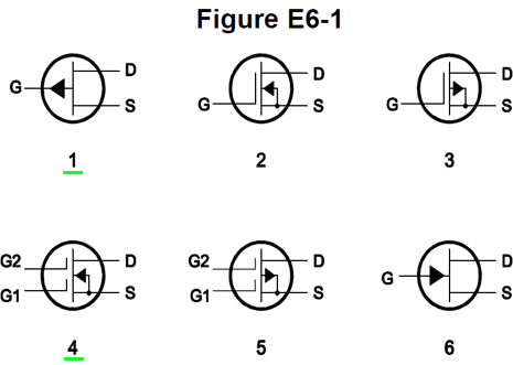
The two "important" ones are on the left. 1 is a P-channel junction FET, with a contact to the gate. 4 is a N-channel dual-gate MOSFET, with the gaps between the metal gates and the body, indicating the silicon dioxide insulating layer in each one. 2 and 3 are standard MOSFETs (N- and P-channel), 5 is P-channel dual-gate MOSFET, and 6 is an N-channel J-JET.
Given there are many variations of FET, you may wish to read the Wikipedia article on FETs.
A power device with a low RDS, or resistance from Drain to Source means a low forward voltage drop, and low dissipation. It is possible to configure one to replace a diode to protect equipment from reverse power connection.
An N-channel MOSFET is likely the best replacement for an NPN to drive a relay, LED, lamp, etc. While no resistor is required between the logic and the gate. However, a high value resistor (eg 1 MΩ) to ground may be required to ensure it is off when it should be, as stray capacitance is enough to hold one on.
An alternative name is "Unipolar Transistor", contrasting with Bipolar Junction Transistor.
This a compound used to make transistors used in UHF, and especially microwave circuits. If you buy a VHF or UHF power amplifier, they may indicate that they include a GaAs-FET pre-amplifier. MMICs (microwave monolithic ICs), and some specialised logic ICs are also made using it.
Gunn Diodes, which generate microwaves, are made from GaAs, and can be used on 10 or 24 GHz bands.
The substance can also be used in space qualified solar cells, and IR LEDs.
Gallium Nitride, which we will discuss in a following page, is a newly exploited material, with lots of microwave and other applications.
Should the concept of amplification be a little abstract, imagine your granny is sitting at the lights in her EV, and a steroid abusing male in a noisy "bloppety-blop-bloppiting" V8, carrying someone he wants to impress, pulls up beside her. The light turns green, she flexes her ankle, the voltage from the accelerator position potentiometer reaching the A to D in the processor swings from 0 to 5 volts, and the motor control system starts sending precisely timed pulses of hundreds of amps at 400 volts to each of the 3 windings, in each of the motors, front and rear. All Mr Roids sees is vanishing taillights. Clearly a lot of loud, profane, raging energy is going to be released within his car, very much greater the the muscular effort of her ankle movement.
I expect you realise one of the more basic forms of diodes is the silicon rectifier or sometimes termed a "power diode". 1N4001 to 1N4007 have a 1 amp rating, and a peak inverse voltage (PIV) of 50 to 1000 volts; the 1N5400 to 1N5408 series is 3 amps. 1N5391 to 1N5399 is a rarer 1.5 amp product in the same family. In each case while low current VF may be 0.6 volts, escalating to 1 volt at the rated current, and higher during higher current pulses, such as charging capacitors during PSU start-up. These are in small black plastic cylinders, larger for larger currents.
European products may have a BY prefix, such as BY127; or BA. Again, this is the Pro Electron system. Japanese items have a 1S prefix. MR often indicates they were introduced by the semiconductor division of Motorola, now ON Semiconductor.
They are also used placed in reverse across relay coils to absorb the energy in the collapsing magnetic field then the current is removed, as the voltage spike can damage the transistor otherwise. Many call this back EMF, but it in fact flows in the same direction as the coil current.
I am sure you are aware that diode bridges to rectify AC to DC can be within a single panel mount case, or through-hole or surface mount package. Four diodes are used for single phase.
Large diodes are designed to be fitted to a heatsink. Some are in 2-pin versions of transistor cases, such as TO-220-2 aka TO-220AC or TO-247-2 aka DO-247; or they mount via stud at the anode or cathode. Bridges may be metal clad, and bolted to a heatsink. Two diodes with a common cathode or common anode can be placed in a TO-220 case, or larger TO-247 or TO-3P case. These form "half bridges". The alternative half bridge is two diodes in series, with 3 terminals exposed, or even two independent diodes in a bolt-down package. 6 diode, 5 terminal bridges rectify 3 phase power, with 3 terminals as the AC inputs, and 2 for the DC output. These are often quarter-inch tabs for push-on terminals, or screws. Hockey Puck diodes carry hundreds to thousands of amps, and need large heatsinks on both sides, and are used in rail traction and welding, along with SCRs in the same style.
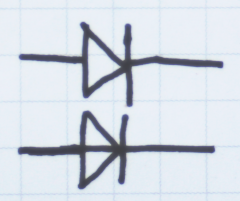
| Excuse the wonkiness. While filled in triangles (item 4 below) are usually used, these two versions are commonly used when designing or drafting a circuit. The lower is handy when you realise you need to insert a diode when you already have a line between other parts, although you can always use a filled one. You can vary the cathode to form a Zener symbol, etc. |
Sustained or recuring high current through a diode will cause the junction to heat, just as current through a resistor causes heating. The increase in VF with an increase in IF can worsen this. P = IF times the actual VF at this current. They are however rugged in terms of handling brief high current pulses.
1N4148 is a switching diode, sometimes termed a signal diode, useful in things like OR gates, or programming devices using a "diode matrix". Its rating 150 mA and 75 volts. The case is a tiny glass cylinder. 1N914 is its close cousin, and high street retailers may supply whichever was cheapest at the market in Guangzhou or Shenzhen a few months ago. 1N916 works too. Symbol 4 below is used for signal diodes too, or the versions above.
Off the exam, how do you determine the required PIV? In the circuit below, if 100 volts AC (RMS) is applied to the capacitor filtered half-wave rectifier, is 100 enough? Surely 200? NO! The capacitor will charge to 100 × √2, or 141.4 volts (or 140.8 once the diode's 0.6 volts is accounted for), while the peak negative voltage of the waveform is also 141.4 volts. Thus at the cathode we have +140.8 volts, and at the anode -141.4 volts, which is 282.2 volts apart: -141.4 - 140.8 = -282.2 volts. Assuming low current, the lowest rated suitable device is the 1N4004 at 400 volts PIV. 1N5394 is a 300 volt, 1.5 amp jobby, but if the mains floats high, or the transformer output is higher than specified due to being lightly loaded, then the voltage imposed will exceed 300 volts.

The waveform is shown on the graph below, 100 volts RMS has plus and minus 141.4 volt peaks.

As an aside, in reality, no matter the number on the package, all modern 1N400x diodes are likely to use the same internals as either a 1N4004, or 1N4007, shown by a small step-up in VF above the 400 volt point, and a tell-tail reduction in capacitance. That said, you should follow the markings, in case you are supplied with New Old Stock devices; prices are likely no or little different.
Note that the 1N4000A is a 7.5 volt, 10 watt stud (bolt) mount Zener diode, so referring to the "1N4000 series" is incorrect, even if most would understand what you meant.
Beyond simple rectifiers, there are many diodes with a range of special features, including for use in RF and microwave circuits.
These are a variation on the regular power rectifier diode, with a low forward voltage drop. This makes the maximum voltage available to the load, but also means the power wasted, and so needing to be dissipated in the diode is lower for a given current. P = IF x VF, so the lower VF the better.
The diode is named for Walter Schottky, as it uses a metal‐semiconductor junction, which forms a "Schottky barrier".
Examples include the 1N58xx series, which have limited reverse voltage characteristics, 20 to 40 volts max; while modern surface mount devices performing better, up to 200 volts. For details of both see: Wikipedia: 1N58xx Schottky diodes
Alternative names are Schottky barrier diode (SBD), or hot-carrier diode. Variations use silicon carbide, with a lower reverse leakage current, but higher forward voltage drop; or Gallium Nitride (GaN).
It is "important" to remember the Schottky is item 6, with right angle bits. Also "important" is that small signal ones are used at VHF and UHF as a mixer or detector. Viewing the photo on Wikipedia: Schottky diode, the devices on blue tape, to the left are small signal RF devices, while the others for power.
A few diodes are in small round white glass beads.
Also off the paper: Another factor is the recovery speed of the rectifier, both forwards and reverse, meaning how fast they commence conducting, and more importantly, how fast they stop conducting, as otherwise reverse current flows. A 1N400x diode will not switch correctly at switchmode frequencies. In June 1995 Electronics Australia had a project which would step up 12 volts to run retail (electronic ballast) compact fluoro lamps, which included a bridge of fast diodes, as at the 75 kHz or whatever frequency it ran at the bridge in the lamp would not have worked. Silicon Chip had one in September 2004, operating at 85 kHz. These are also termed Fast Recovery Rectifiers, and there are also ultrafast diodes. EA specified BA159 or MR856.
GaN (Gallium nitride) has wide application, up to military radar, which operates at microwave frequencies. It is used as a selling point on for 'phone / tablet chargers. The implied or claimed benefit is a greater power output in a smaller size, and questionable claims of faster charging. They do run hot! There is a suggestion they could replace magnatrons in microwave ovens, no doubt initially at a premium price point, and/or for niche uses.
Silicon Carbide (SiC), and Silicon Germanium (SiGe) are further new materials. An example Silicon Germanium Schottky diode, suitable for post-transformer rectification and similar applications is the PMEG120G30ELP. I used them on the copper side Vero board by it joined the first and third strips, optionally removing a portion of the second strip. The rating is 120 volts and 3 amps. VF is a 700 mV at 1 amp, a little lower than a 1N400x series. Some of the half-bridge devices listed by RS or Element 14 / Farnell are SiC.
Standard or Schottky diodes can also be used to direct current flow - after all thermionic diodes were termed "valves", at least by the Brits, as they acted like a one-way valve. Before flash memory was available one way to keep settings in a PC or test equipment was to use a soldered in 3.6 volt Lithium Thionyl Chloride primary cell, typically of AA size. A diode from the supply rail to the memory, and from the cell to the memory are used. These cells have exploded in the past, one very large one fatally, so in some case two diodes were used from the cell as a precaution, to prevent unintended attempted charging. These also prevent the cell attempting to power other parts of the device. When there is 5 volts available this powers the memory, preventing discharge of the cell.
Modern CMOS ICs are often protected by internal diodes placed to shunt excessive positive charges to the positive rail, and negative voltages to ground. Data sheets usually caution against applying an input more than 0.5 volts outside the rails, as these diodes have limited ability to dissipate power.
One or more in series with a circuit is also a convenient way to reduce a voltage by a volt or two.
A 1N4001 or similar diode can be placed from output to input of a 78xx or LM340 voltage regulator to protect the regulator from a short on the input side causing current to flow from the output capacitor via the internal current pass device.
You can also use them to increase the output of a 78 series regulator. Two from IC ground to circuit ground on a 7805 should give about 6.2 volts out if you can't find a 7806. You need a 2.2 kΩ) resistor from output to its Gnd terminal. A reverse biased Zener can do this too.
Oh dear, searching for a rare part number I somehow came across lunatics who think that looping diodes legs and putting them on skin reduces pain from serious illnesses. Utter quackery! And more likely to cause minor lead absorption than anything else.
Remembering back to the Technician paper, these were used in a power supply as a simple "shunt" voltage regulator. The symbol is in item 3 above, with 45 degree elements off the bar. One with only a short right angle bar back over the arrow part was used in Britain, or one with a reversed L left of the upwards pointing diode is used in Funway 2 (see below).
The characteristic which make this work is that the voltage remains fairly constant over a range of reverse currents, although there is a slight upwards trend. If the current is forwards the drop us around 0.6 volts, similar to a regular silicon diode.
While the most common use is as a shunt regulator, as a voltage reference for a discrete regulator, or (for large ones) as protection in case a power supply goes over-voltage, the other option is to use it as a voltage dropping component, termed a level shifter. Thus a 24 to 28 volt range passing through a reverse biased 16 volt zener becomes an 8 to 12 volt range out.
This simple circuit detects when a voltage is above about 19 volts, and is designed to indicate if a lighter outlet is supplying 24 volts (or 28 if the engine is running), rather than 12 volts. A 15 or 16 volt Zener is used, so unless the voltage is well above 14 volts, the LED won't light. If the voltage is 24 - 30 volts, then around 0.6 volt is dropped in the first diode (there in case the polarity is reversed), 15 or 16 volts is dropped in the Zener, and 2 or 3 in the LEDs. The resistor is selected so the current is 20 mA with 28 volts on the circuit. The power is 16 v x 20 mA = 320 mW, so best to use a 1 watt, rather than 400 mW Zener if the device is to remain connected for any significant period.

For a 16 volt zener use a 470 ohm resistor, of more than a quarter watt if used for more than a moment. For 15 volts use 510 ohms, half watt. You could likely use a constant current diode within it ratings. You can also put it across the DC terminals of a bridge to make it dual polarity (remove the protection diode). You could add a separate circuit with a bi-colour / tri-colour LED (inverse parallel LEDs in one package) and resistor to indicate polarity, including when 12 volts is present. Or replace D1 with another Zener, and the LED with a tri-colour LED or individual LEDs in inverse parallel. (Tri-colour here means that low voltage AC produces the appearance of a yellowish light, rather than just the red or green. This is different to to a multipin RGB LED). You could make this in surface-mount or on a small through-hole PCB, and connect it to whatever connector style you use for field power. You could also solder it together, perhaps with the resistor in the negative leg, and heatshrink each leg.
Part numbers include 1N4728A to 1N4761A and 1N5221 to 1N5267, apparently 1 watt and 400 mW; digits being merely sequential, with no direct indication of value. BZ is the European prefix, with an example range being BZX85C3V3 to BZX85C75, with voltages ranging from 3.3 to 75 volts, the V being the decimal, just as a resistor can be 4k7 for 4.7 kΩ. The permitted dissipation chart suggests they would be termed 1 watt in hobbyist listings.
The alternative to "Zener breakdown" used here is "Avalanche breakdown" which occurs in avalanche diodes. Note that ordinary power diodes undergoing reverse breakdown can suffer hotspots, and thus be damaged. Transient voltage suppression diodes (TVS diodes) are used to suppress fast rising, short duration high voltage pulses, including under the brands Transzorb and Transil.
When LEDs are forward biased, they emit visible, IR, or UV light. While the spectrum may not be particularly narrow, they do appear as pure colours. Standard LEDs have a forward voltage drop of 1.8 (red) to around 4 volts, depending on the material used, and therefore the colour. High efficiency / super / ultra / hyper red drop 2.2 volts; and old style yellowish green ones drop about 2.2 volts, with modern pure and bluish greens, around 3. In older papers IR LEDs are termed IREDs, infra-red emitting diodes, as used in remote controls, and now illumination for paranoia cameras, and invasive and potentially unlawful face recognition (Bunnings and Kmart got busted for this). Green gas welding glasses appear to block IR, and prevent these working, as can face masks.
The exact colour of LEDs are specified by wavelength, expressed in nanometres. For commercial users LEDs can be "binned" by exact colour (wavelength) and brightness for consistent appearance, while AliExpress sellers and Jaycar sell what is left over. I expect a bag or LEDs from RS / E14, etc would contain consistent parts for a bargraph, etc. Brightness, in millicandela (mCd) and the angle of illumination are also specified, with some oval rather than round.
Standard LEDs are typically driven with a DC voltage, via a current limiting resistor. R = (VS-VF)/I, say 15 mA on a 13.8 volt supply: R = (13.8-2.2) / 0.015 = 11.6 / 0.015 = 773.333333333333. 750, 787, or 820 are suitable values. 777 ohms is available, but rare. Power = 11.5 × 0.015 = 0.1725 W. A 400 mW or a half-watt resister is preferable, for reliability.
Where a resistor has current flowing continuously, or with a high duty cycle, it is usual to use a resistor with a rating of at least twice the power dissipated by it, to prevent it becoming excessively hot. The DALE mil-spec items with printed values are very conservatively rated, so use at the marked value is fine. They are now made by Vishay.
The latest question on them discusses the band gap, which is the feature of the material which causes LEDs to emit. This determines the forward voltage drop, VF, and as this increases (and so the band gap energy also increases) the colour changes from IR to red, then amber / orange, then yellow through greens to blue, and eventually to violet, and several UV wavelengths. Special "dental blue" LEDs cure resin composite fillings, typically using 460 nm light. There are also cyan, torquise, and lime LEDs.
Note that this is a characteristic of the material, and attempting to apply a higher voltage does not alter the colour.* There is an online video showing an orange or yellow LED glowing green when dipped in liquid nitrogen, but that is an extreme situation. Industrial or research diode lasers can be tuned by chilling them.
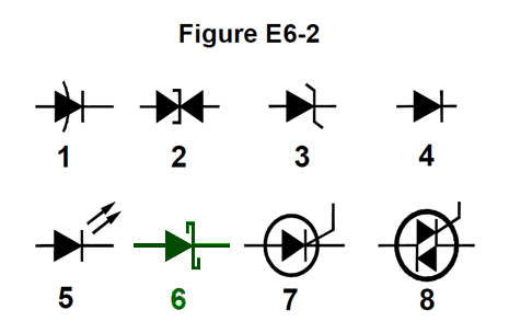
The LED symbol is item 5, with outwards pointing arrows indicating photons. Both Australian, "Dick Smith's Funway into Electronics" series and Silicon Chip magazine used / uses a diode symbol including a lower case lambda, λ, the symbol for wavelength. SC's articles appearing in the British EPE and Practical Electronics use this too, the local items the arrow version. LEDs or combinations of LEDs in one device may be circled. Unfortunately Dick has now been captured by the anti-clean energy movement, or his fossil fuel investments are speaking.
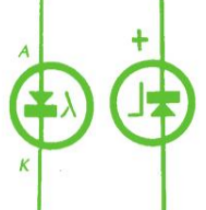 | As used in some Australian publications, an LED and a Zener, taken from the introductory pages of Funway 2. No, they are were not drawn entirely straight. |
Off the exam, inwards pointing arrows indicate a photodiode, which is a light or IR sensor. A lot of entertainment equipment includes a three pin device which integrates an IR sensitive diode with an amplifier and demodulator to receive remote control commands.
Since around 2000 there have been both 20 mA and high current blue LEDs with a yellow phosphor, which output what appears to be white light. These can replace incandescent lamps in many situations. These can be used as light for field operations, perhaps two or 3 in series with a suitable power resistor, across 12 volts. 1 watt units typically use 300 mA; 3 watt ones, around 1 amp. These must be attached to a heatsink of some sort. There are also COB, with one, or usually many LED dies (chips) directly connected to the board, and the phosphor as a coating over the whole board. Often a switching arrangement is used, but this can risk generating interference.
The large "star" LEDs are also available in colours such as red and amber, like normal LEDs. Phosphor based devices provide a stronger, brighter yellow than traditional types. Pink devices use a phsophor, as do various plant growth lamp LEDs, and yes, some are used for legal crops. "Peach" and "raspberry" are a couple of less comon colours. There appear to be purple ones which are not UV LEDs.
Note that the package of an LED should NOT be considered to provide isolation from mains or other dangerous voltages. Circuits which use capacitive reactance to limit current in LEDs can be subject to breakdown (shorting) of capacitors not specifically marked for mains use.
*The exception is the Q-Pixel brand polychromatic microLED displays made from GaN, where the voltage applied to the tiny pixel determines the colour! Like ICs they are made in a monolithic process. They are being promoted for use in extremely fine pitch displays, in goggles, view finders, and weapon sights.
These consist of P-type, undoped Intrinsic material, and N-type. These result in a large gap, and so low capacitance. They are thus useful as an RF switch or attenuator.
Often a standard diode symbol is used, although there is a version with an wedge in an extended area between the triangle and bar. The DC bias voltage is typically fed via an inductor (choke) and a resistor. They can also be used to protect input stages from large signals.
When used as an attenuator they are placed with other components so that they shunt the signal, under the control of a varying forwards DC voltage, with an increased voltage increasing the attenuation. They can also be used as a modulator for microwave signals.
They can form shunt or series SPST switches, or complex combinations. Reading this guide (or at least viewing the diagrams) is worthwhile: PIN Diode Handbook from the Long island, not Liechtenstein, branch of the IEEE, despite the .li domain.
Series switching works by using a grounded inductor on the cathode side while feeding DC into the anode side, also via a coil, as in the guide above.
All diode junctions, and especially those reverse biased have some capacitance, as they consist of layers of conductive material with a layer of low or non-conductiing material between them. The Varactor is designed to take advantage of this. At low bias the typical device for a video tape recorder's tuner (BB639 or BB659) has around 30 pF at low bias, while at high bias (25 v) it may be 2.5 pF. BB202 does 30 to 5 pF, but only needs 5 volts to minimise the capacitance, so is fine in battery FM radios. One brand was "Varicap", now in common use. The symbol, a diode with a double bar, (capacitor symbol) on its nose, along with typical circuit configurations are shown here: Wikipedia: Varicap
One question lists two interesting kinds of rectifiers as incorrect answers.
One is the Thermionic emission diode, alluding to diode valves or tubes. These were used as power rectifiers for various valve electronics, and included dual anode versions which were used as full-wave (not bridge) rectifiers.
The Cat's whisker or crystal detector most often used Galena, being Lead sulfide (PbS) with a fine, springy Phosphor bronze wire coming down from an arm. Silicon was another material. Requiring a clamp to provide high pressure, Carborundum was used in professional radiotelegraphy stations. Its chemical name is silicon carbide (SiC), so everything old is new again. This material however required a battery to bias the junction.
Electrolytic rectifiers are rarely, if ever used now, but you can build one at home. They consist of a electrodes consisting of lead and aluminium (aluminum) in a solution of Sodium Carbonate (washing soda); and alum, meaning Potassium alum. Note the lead is be toxic, and other items may be too. Link. These concepts however led to the electrolytic capacitor.
The Electrolytic detector looks like a Galena cat whisker detector, but uses a extremely fine platinum wire in a tiny lead or platinum pot of nitric acid.
While there are tricks to allow a FET with a low RDS in place of a series "idiot diode", to protect equipment for reverse polarity, with a lower forward drop, these are NOT diodes.
Off the exam, but interesting, are Selenium rectifier stacks. These have high forward voltage drops, so care needs to be taken if replacing these with modern devices, lest the supplied circuit be supplied with an excessive voltage. This also meant that power dissipation was high, so there they included large discs or squares of steel or aluminium for heatsinking, as well as acting as the substrate. These are infamous for generating a REALLY nasty smell (toxic hydrogen selenide gas) when they burn out. A "sickly sweet" smell indicates that they are at end of life, and conducting in reverse too. They were used for low speed logic gates in early computers, as diodes in the form of 3.175 mm discs could be punched from a sheet at a cost much less than silicon diodes.
The even earlier form of metal rectifier was the copper oxide rectifier. Mercury-arc and argon rectifiers are both plasma rectifiers. In the early 20th century NSW railways generated their own power at 25 Hz, and used mechanical rectification, using a synchronous motor and rotating contacts to convert it to DC for rail power.
By chance, another semiconductor developer was named William Shockley, hence the Shockley "diode", a now depricated 4 layer device. It is an two terminal voltage based trigger device, replaced by the dynistor, and not to be confused with the Schottky diode.
Off the exam: The constant-current diode (aka current-limiting diode (CLD) aka current-regulating diode (CRD)) limits current to to a specific level. Many are in the units of milliamps range, but 100 μA to 500 mA are available. They are often used to set up conditions in an amplifier, A to D, or similar circuit. They can also be used to power LEDs, especially under varying input voltage situations. Many are really a simple IC containing a FET and resistor.
Likewise off the exam, Tunnel Diodes were an early but interesting device, a thing of legend when I was at school. They are said to have a negative differential resistance region, where they can be used as RF amplifiers, in oscilators, as well as being the triggering elements in oscilloscopes, and as RF switches. However, 3 pin devices have replaced them. Note that "negative resistance" is NOT a correct answer, despite Gunn Diodes also using the phenomena. Gas discharge tubes, such as neons exhibit this too, where the voltage across them drops after they strike.
1 is a variable voltage diode. 7 and 8 are the silicon controlled rectifier and the triac, both used in things like lamp dimmers, and other power control systems. I can't find 2 online, but it is similar to a bidirectional transient-voltage-suppression (TVS) diode.
Discharge of static electricity, especially through MOS / CMOS devices can blow a hole in the thin insulating silicon oxide layer, destroying the device, or damaging it so it fails later. This latent damage issue also applies to equipment which apparently survives a lightning strike. High performance LEDs are also susceptible to static damage.
While working with such equipment, it is wise to wear a static dispersing wrist-strap, and to work on a good quality static dissipative desk mat. These are grounded via a high value resistance, selected so if you do touch a mains voltage while wearing one the current through your body via the strap is limited to a safe level.
It can also change the value of precision resistors. This was discovered early in the space programme, when resistors from Britain arrived with values significantly different to when they were sent. From memory there were tracks of conductive material between the spirals of metal film, causing a step change in value. After a great deal of puzzlement by the team an engineer's wife asked if it was the packaging. It was! This was at a time when oil derived plastics were replacing things like waxed or other paper, and Cellophane made from cellulose (although this can become charged too).
Parts and assembled boards should be stored in nickel coated plastic bags, those made from pink colour-coded antistatic plastic, or from carbon-loaded black plastic, as specified. There are antistatic foams, and small cardboad boxes coated in a carbon-loaded ink. Storage tubs, tools and pens made from carbon loaded plastic are also avaliable, along with pink plastic waste bin liners. Specific clothing is worn while working in commercial situations, but otherwise cotton in preferable to nylon or polyester.
These are the actual questions from the Extra licence exam pool, as published by the NCVEC.
E6A01
In what application is gallium arsenide used as a semiconductor material in preference to germanium or silicon?
A. In high-current rectifier circuits
B. In high-power audio circuits
C. In microwave circuits
D. In very low frequency RF circuits
GaAs devices are used at microwave and UHF frequencies, answer C.
E6A02
Which of the following semiconductor materials contains excess free electrons?
A. N-type
B. P-type
C. Bipolar
D. Insulated gate
N type, N standing for negative has excess free electrons, remembering electrons are negatively charged, answer A.
E6A03
Why does a PN-junction diode not conduct current when reverse biased?
A. Only P-type semiconductor material can conduct current
B. Only N-type semiconductor material can conduct current
C. Holes in P-type material and electrons in the N-type material are separated by the applied voltage, widening the depletion region
D. Excess holes in P-type material combine with the electrons in N-type material, converting the entire diode into an insulator
The active parts of the P and N materials are separated by a widened depletion layer, answer C.
E6A04
What is the name given to an impurity atom that adds holes to a semiconductor crystal structure?
A. Insulator impurity
B. N-type impurity
C. Acceptor impurity
D. Donor impurity
Holes can accept current, so are the result of an acceptor impurity, answer C.
E6A05
How does DC input impedance at the gate of a field-effect transistor (FET) compare with the DC input impedance of a bipolar transistor?
A. They are both low impedance
B. An FET has lower input impedance
C. An FET has higher input impedance
D. They are both high impedance
FETs have significantly higher input impedance, answer C.
E6A06
What is the beta of a bipolar junction transistor?
A. The frequency at which the current gain is reduced to 0.707
B. The change in collector current with respect to the change in base current
C. The breakdown voltage of the base-to-collector junction
D. The switching speed
If an increase of 1 mA in current goign into the base causes and increase of 100 mA to the flow into the collector, then the beta (β) is 100, so answer B.
E6A07
Which of the following indicates that a silicon NPN junction transistor is biased on?
A. Base-to-emitter resistance of approximately 6 to 7 ohms
B. Base-to-emitter resistance of approximately 0.6 to 0.7 ohms
C. Base-to-emitter voltage of approximately 6 to 7 volts
D. Base-to-emitter voltage of approximately 0.6 to 0.7 volts
The key terms are silicon, meaning a voltage of 0.6 to 0.7 volts; and that the base to emitter junction is a PN junction, as indicated by the last two letters, so the voltage is positive between the base and emitter. Thus VBE is 0.6 to 0.7 volts, turning the device on, answer D.
E6A08
What is the term for the frequency at which the grounded-base current gain of a bipolar junction transistor has decreased to 0.7 of the gain obtainable at 1 kHz?
A. Corner frequency
B. Alpha rejection frequency
C. Beta cutoff frequency
D. Alpha cutoff frequency
This is the Alpha cutoff frequency, answer D.
RF amplifiers may ground the base, rather than use it as the input terminal in some RF circuits. Alpha is a way of comparing the change of collector current with respect to emitter current.
E6A09
What is a depletion-mode FET?
A. An FET that exhibits a current flow between source and drain when no gate voltage is applied
B. An FET that has no current flow between source and drain when no gate voltage is applied
C. An FET that exhibits very high electron mobility due to a lack of holes in the N-type material
D. Any FET for which holes are the majority carriers
It is a FET which requires a voltage to constrict the current flow, answer A.
E6A10
In Figure E6-1, what is the schematic symbol for an N-channel dual-gate MOSFET?
A. 2
B. 4
C. 5
D. 6
In symbol 4, the isolation of the gates from the channel indicates it is a MOSFET, and the inward pointing arrow that the channel is made from N material, answer B.
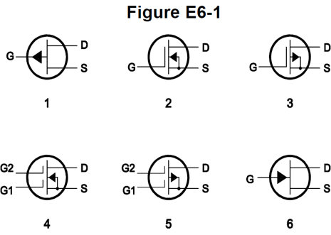
E6A11
In Figure E6-1, what is the schematic symbol for a P-channel junction FET?
A. 1
B. 2
C. 3
D. 6
In symbol 1, the connection of the gate to the channel indicates it is a junction FET, and the outward pointing arrow that the channel is made from P material, answer A.
E6A12
What is the purpose of connecting Zener diodes between a MOSFET gate and its source or drain?
A. To provide a voltage reference for the correct amount of reverse-bias gate voltage
B. To protect the substrate from excessive voltages
C. To keep the gate voltage within specifications and prevent the device from overheating
D. To protect the gate from static damage
The gate insulation is a thin layer, typically of silicon oxide. If you touch older MOSFETS or older CMOS ICs without using static protection, there is every chance you will damage the device, due to static discharge from your body to the device, blowing a tiny hole in this insulation layer, answer D.
The Zener diode(s) can generally dissipate this energy safely. It may be built into the MOSFET package. Note that if you build a PC without wearing a wrist-strap, it may work fine now, but may well fail in a few months.
E6B01
What is the most useful characteristic of a Zener diode?
A. A constant current drop under conditions of varying voltage
B. A constant voltage drop under conditions of varying current
C. A negative resistance region
D. An internal capacitance that varies with the applied voltage
As the current through the device varies, the voltage stays (fairly) constant, answer B.
E6B02
Which characteristic of a Schottky diode makes it a better choice than a silicon junction diode for use as a power supply rectifier?
A. Much higher reverse voltage breakdown
B. More constant reverse avalanche voltage
C. Longer carrier retention time
D. Less forward voltage drop
These have a lower forward voltage drop, and so lower power dissipation, answer D.
E6B03
What property of an LED's semiconductor material determines its forward voltage drop?
A. Intrinsic resistance
B. Band gap
C. Junction capacitance
D. Junction depth
Each material combination has a specific band gap which alters the forward voltage, answer B. And the colour.
E6B04
What type of semiconductor device is designed for use as a voltage-controlled capacitor?
A. Varactor diode
B. Tunnel diode
C. Silicon-controlled rectifier
D. Zener diode
Varying the negative bias on a varactor diode effectively varies the distance between the plates of the capacitor formed by the diode elements in their non-conducting state. Bog standard diodes also exhibit this effect to some degree, but varactors are designed to maximise it, answer A.
If you had a VHS or maybe a Beta machine with small multi-turn adjustable resistors (trim-pots) to set each channel, then I expect these were selectively connected to a varactor in the tuner, to select the TV channel to watch or record.
E6B05
What characteristic of a PIN diode makes it useful as an RF switch?
A. Extremely high reverse breakdown voltage
B. Ability to dissipate large amounts of power
C. Reverse bias controls its forward voltage drop
D. Low junction capacitance
The large band of undoped or intrinsic material, means it has low capacitance, answer D.
E6B06
Which of the following is a common use of a Schottky diode?
A. In oscillator circuits as the negative resistance element
B. As a variable capacitance in an automatic frequency control circuit
C. In power supplies as a constant voltage reference
D. As a VHF/UHF mixer or detector
These are used at VHF and UHF as a mixer or detector, answer D
These are also termed Hot carrier diodes, and use can extend into the microwave range.
E6B07
What causes a junction diode to fail from excessive current?
A. Excessive inverse voltage
B. Excessive junction temperature
C. Insufficient forward voltage
D. Charge carrier depletion
As with a resistive component, or even a wire, excessive current causes excessive heating of the diode's junction, leading to failure, answer B.
Standard power diodes can survive brief pulses much greater than their rated current, but if an excessive current is maintained for a period, they will fail.
E6B08
Which of the following is a Schottky barrier diode?
A. Metal-semiconductor junction
B. Electrolytic rectifier
C. PIN junction
D. Thermionic emission diode
This is a metal to semiconductor junction, answer A.
E6B09
What is a common use for point-contact diodes?
A. As a constant current source
B. As a constant voltage source
C. As an RF detector
D. As a high-voltage rectifier
These are used as an RF detector, including in modern "crystal sets", a basic AM receiver, answer C.
While the radio without local power is a cool trick, a 1.5 volt cell from a flashlight / torch or old fashioned crank 'phone was used in many improvised "fox-hole" radios. They can also be used after amplifier stage(s), such as in the Tuned Radio Frequency (TRF) receiver design, although a diode valve / tube was often used.
E6B10
In Figure E6-2, which is the schematic symbol for a Schottky diode?
A. 1
B. 6
C. 2
D. 3
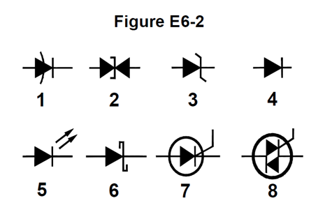
The right angle parts folded back on themselves in symbol 6 indicate a Schottky diode, answer B.
E6B11
What is used to control the attenuation of RF signals by a PIN diode?
A. Forward DC bias current
B. A variable RF reference voltage
C. Reverse voltage larger than the RF signal
D. Capacitance of an RF coupling capacitor
This is forward DC current, answer A.
The other use for a standard or Schottky diode is as an idiot diode, in series with a circuit, in case a 9 volt battery is touched to the terminals backwards, or banana plugs are placed backwards. The alternative method is to put a diode backwards across the circuit, which avoids the voltage drop, but which MUST be used with a fuse. A power Zener or TVS can also be used.
Thinking in the shower: After adjusting the taps there is a delay of a few seconds before the temperature changes - latency!.
On to: Components 2 - Logic ICs, PLDs, Inductors, & Piezoelectric devices
You can find links to lots more on the Learning Material page.
Written by Julian Sortland, VK2YJS & AG6LE, January 2026.
Tip Jar: a Jefferson (US$2), A$3 or other amount / currency. Thanks!
You can also buy me a non-coffee beverage: ko-fi.com/ag6le